用于FPGA的高吞吐量通道器
此示例显示如何通过使用多相滤波器库来实现高吞吐量(每秒GIGASAMPLE,GSP)信道,用于硬件。
High speed signal processing is a requirement for applications such as radar, broadband wireless and backhaul.
Modern ADCs are capable of sampling signals at sample rates up to several Gigasamples per second. But the clock speeds for the fastest FPGA fall short of this sample rate. FPGAs typically run at hundreds of MHz. An approach to perform GSPS processing on an FPGA is to move from scalar processing to vector processing and process multiple samples at the same time at a much lower clock rate. Many modern FPGAs support the JESD204B standard interface that accepts scalar input at GHz clock rate and produces a vector of samples at a lower clock rate.
In this example we show how to design a signal processing application for GSPS throughput in Simulink. Input data is vectorized through a JESD204B interface and available at a lower clock rate in the FPGA. The model is a polyphase filter bank which consists of a filter and an FFT that processes 16 samples at a time. The polyphase filter bank technique is used to minimize the FFT's inaccuracy due to leakage and scalloping loss. SeeHigh Resolution Spectral Analysis(DSP System Toolbox) for more information about the polyphase filter bank.
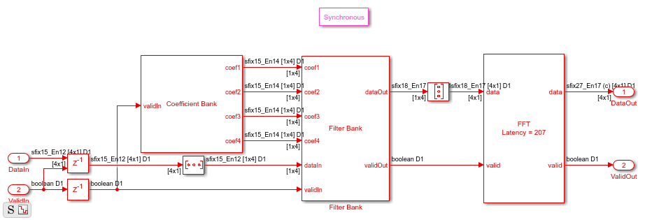
该first part of the example implements a polyphase filter bank with a 4-tap filter.
该second part of the example uses the Channelizer HDL Optimized block configured for a 12-tap filter. The Channelizer HDL Optimized block uses the polyphase filter bank technique.
多相过滤银行
modelname =.'PolyphaseFilterBankHDLExample_4tap';Open_System(ModelName);
该InitFcn回调(模型属性>回调> initfcn)设置模型。该模型使用512点FFT,每个频带都有四个抽头滤波器。使用dsp.HDLChannelizer系统对象™生成系数。通道器对象的多相方法产生512×4矩阵。每行代表每个频带的系数。将系数铸造成具有与输入信号相同的字长的固定点。
FFTLength = 512; h = dsp.Channelizer; h.NumTapsPerBand = 4; h.NumFrequencyBands = FFTLength; h.StopbandAttenuation = 60; coef =fi(polyphase(h),1,15,14,'RoundingMethod'那'Convergent');
该算法需要512个过滤器(每个频带的一个过滤器)。对于16个样本的向量输入,我们可以重用16个过滤器,32次。
八大= 16;重新使用= fftlength / eng;
To synthesize the filter to a higher clock rate, we pipeline the multiplier and the coefficient bank. These values are explained in the "Optimized Hardware Considerations" section.
Multiplication_PipeLine = 2; CoefBank_PipeLine = 1;
Data Source
输入数据包括两个正弦波,200 kHz和250 kHz。
仿真结果
To visualize the spectrum result, open the spectrum viewers and run the model.
open_system('PolyphaseFilterBankHDLExample_4tap/FFT Spectrum Viewer/Power Spectrum viewer (FFT)');open_system('PolyphaseFilterBankhdlexample_4TAP / PFB频谱查看器/功率谱查看器(PFB)');sim(modelname);

多相滤波器组功率谱观察器显示了与仅使用FFT相比的功率谱和频率泄漏和扇形最小化的改善。通过比较两个频谱,并在100 kHz和300 kHz之间进行变焦,观察到多相滤波器组比经典FFT超过-40 dB的峰值较少。
Optimized Hardware Considerations
Data type:数据字长度影响结果的准确性和硬件中使用的资源。对于此示例,我们以完整的精度设计过滤器。输入数据类型
Fixdt(1,15,13)那the output isfixdt(1,18,17)。滤波器系数的绝对值均小于1,因此每个乘法后数据不会生长,并且我们需要为每个添加添加一位。为了保持FFT的准确性,我们需要为每个阶段生长一位。这使得在每个阶段更大的旋转因子倍增。对于许多FPGA,希望保持小于18x18的乘法大小。由于512点FFT具有9个阶段,因此FFT的输入不能超过11位。通过探索过滤器系数,我们观察到最大系数的前8个二进制数字为零,因此我们可以将系数施放到fixdt(1,7,14)代替fixdt(1,15,14)。此外,我们观察到,多相滤波器库内的数据类型块输出的最大值在二进制点之后具有7个前导零,因此我们将滤波器输出施放到fixdt(1,11,17)instead. This keeps the multiplier size inside the FFT smaller than 18-by-18 and saves hardware resources.
设计速度:
国家控制块:State Control块以同步模式使用,为带有启用端口的延迟块生成硬件友好代码。
最小化时钟使能:该模型设置为生成HDL代码,最小化时钟启用选项打开(在配置参数中,选择> HDL代码生成>全局设置>端口>最小化时钟启用)。当模型是单速率时,支持此选项。万博1manbetx时钟启用是一个全局信号,不推荐用于高速设计。
Usage of the DSP block in FPGA:In order to map multipliers into a DSP block in the FPGA, the multipliers should be pipelined. In this example we pipeline the multipliers (2 delays before and 2 delays after) by setting Multiplication_PipeLine = 2; These pipeline registers should not have a reset. Set the reset type to none for each pipeline (right-click the Delay block and select HDL Code > HDL Block Properties > Reset Type = None).
在FPGA中使用ROM:Coefficient block inside the Coefficient Bank is a combinatorial block. In order to map this block into a ROM, add a register after the block. The delay length is set by
CoefBank_PipeLine。Set the reset type for these delays to none (right-click the Delay block and select HDL Code > HDL Block Properties > Reset Type = None).
Generate HDL Code and Test Bench
You must have an HDL Coder™ license to generate HDL code for this example model. Use this command to generate HDL code. systemname = 'PolyphaseFilterBankHDLExample_4tap/PolyPhaseFilterBank'; makehdl(systemname);
Use this command to generate a test bench that compares the results of an HDL simulation against the Simulink simulation behavior. makehdltb(systemname);
Synthesis Results
使用ISE为Xilinx Virtex 7(XC7VX550T-FFG1158,速度等级3)合成设计。该设计实现了499.525 MHz(在地方和路线之前)的时钟频率。在每个时钟的16个样本中,这转化为8 GSP吞吐量。请注意,此子系统具有大量I / O端口,并且它不适合作为针对FPGA的独立设计。
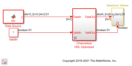
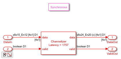
HDL Optimized Channelizer
为了提高频率响应,使用具有更多抽头的过滤器。以下模型使用通道器HDL优化块,配置有12个抽头滤波器来改善频谱。使用内置的通道器HDL优化块使得更容易更改设计参数。
modelname =.'PolyphaseFilterBankHDLExample_HDLChannelizer';Open_System(ModelName);

该model uses workspace variables to configure the FFT and filter. In this case, the model uses a 512-point FFT and a 12-tap filter for each band. The number of coefficients for the channelizer is 512 frequency bands times 12 tap per frequency band. Thetf(h)method generates all the coefficients.
八大= 16;FFTLength = 512; h = dsp.Channelizer; h.NumTapsPerBand = 12; h.NumFrequencyBands = FFTLength; h.StopbandAttenuation = 60; coef12Tap = tf(h);
Data Source
输入数据包括两个正弦波,200 kHz和206.5 kHz。频率比第一示例更靠近彼此,以说明在频谱分辨率中的信道器和4抽头滤波器之间的差异。
仿真结果
To visualize the spectrum result, open the spectrum viewers and run the model.
open_system('PolyphaseFilterBankHDLExample_HDLChannelizer/PFB_4tap Spectrum Viewer/Power Spectrum viewer (PFB_4tap)');open_system('PolyphaseFilterBankHDLExample_HDLChannelizer/Channelizer Spectrum Viewer/Power Spectrum viewer (Channelizer_12tap)');sim(modelname);
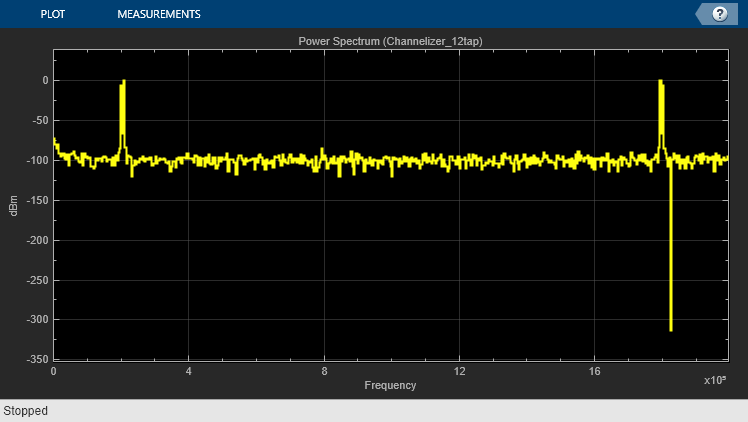
该Power Spectrum Viewer for the Channelizer_12tap model shows the improvement in the power spectrum of the polyphase filter bank with 12-tap filter compared to the 4-tap filter in the previous model. Compare the spectrum results for the channelizer and 4-tap polyphase filter banks. Zoom in between 100 KHz and 300 KHz to observe that the channelizer detects only two peaks while the 4-tap polyphase filter bank detects more than 2 peaks. Two peaks is the expected result since the input signal has only two frequency components.