Measuring Offset and Gain Errors in ADC
This example shows how offset error and gain error are calculated and how each affects the transfer curve of an ADC. Offset error and gain error characterize part of the linearity error in an ADC.
Offset error is the difference between the center of the least significant code and the center of the same code on an ideal ADC with the same number of bits. Offset error is usually reported in units of the least significant bit (LSB) of the converter. One LSB is equivalent to the converter's quantization interval.
在LSB我增益误差s the difference between the center of the most significant code after offset error correction and the center of the same code on an ideal ADC with the same number of bits.
Due to the difficulty in determining the precise location of the center of a code with a non finite boundary, these values are most commonly measured with respect to the first and last threshold of the converter, respectively.
Units for Offset Error and Gain Error
The unit , which is used in this example, is defined as:
![$$1 \left[LSB\right] = \frac{FSR}{2^{N_{bits}}}$$](http://www.tianjin-qmedu.com/help/examples/msblks/win64/OffsetErrorAndGainErrorExample_eq03040517944108971677.png)
Thus, an error in (volts) translates intoas follows:
![$$E \left[LSB\right] = 2^{N_{bits}}\frac{E \left[V\right]}{FSR
\left[V\right]}$$](http://www.tianjin-qmedu.com/help/examples/msblks/win64/OffsetErrorAndGainErrorExample_eq17765393088561812046.png)
where is the full scale range of the ADC and
 is the number of bits of the ADC.
Linearity errors are also commonly reported in normalized units with respect to the full scale range:
![$$ E_{Offset} = \frac{E_{Offset} \left[V\right]}{FSR \left[V\right]}$$](http://www.tianjin-qmedu.com/help/examples/msblks/win64/OffsetErrorAndGainErrorExample_eq14658918440880292589.png)
Another unit sometimes used for linearity errors used is percent full scale. Percent full scale is defined as normalized units multiplied by 100:
![$$E_{Gain} \left[\%\right] = 100\frac{E_{Gain} \left[V\right]}{FSR
\left[V\right]}$$](http://www.tianjin-qmedu.com/help/examples/msblks/win64/OffsetErrorAndGainErrorExample_eq07830225028056899942.png)
Calculate Offset Error and Gain Error
Use a 3-bit ADC with dynamic range [-1 1]. Define an offset error of1LSB and a gain error of1LSB.
Nbits = 3; Range = [-1 1];% ADC Full Scale RangeOffsetError = 1; GainError = 1; LSB = (max(Range) - min(Range)) / (2^Nbits - 1);
The digital codes from the ideal ADC are identical to those from the experimental ADCs.
[TC0Analog, TC0Digital] = og2tc(Nbits, Range, 0, 0);% Ideal ADC Transfer CurveTC1Analog = og2tc(Nbits, Range, OffsetError, 0);% Offset Error OnlyTC2Analog = og2tc(Nbits, Range, 0, GainError);% Gain Error OnlyTC3Analog = og2tc(Nbits, Range, OffsetError, GainError);% Both Offset Error and Gain ErrorplotAdcTcForExample(TC0Digital, TC0Analog, TC1Analog, TC2Analog, TC3Analog, Nbits);
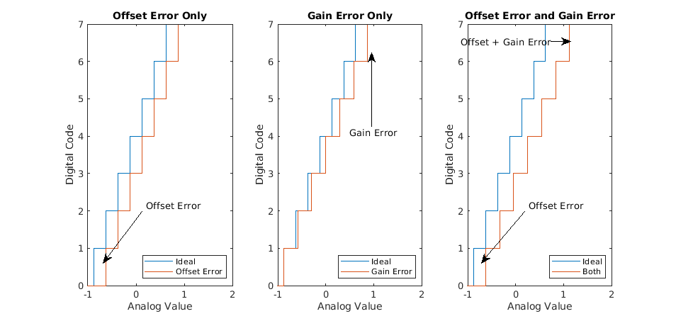
The sum of offset error and gain error is known as full-scale error. In monopolar converters zero error, essentially offset error defined at analog level0, is identical to regular offset error. In bipolar converters such as those above, offset error and zero error are different quantities.
Use of Linearity Errors as Impairments
比较一个flash ADC与偏置和增益误差one with no impairments.
model ='OffsetGainExample'; open_system(model); open_system([model'/Time Scope']); sim(model);
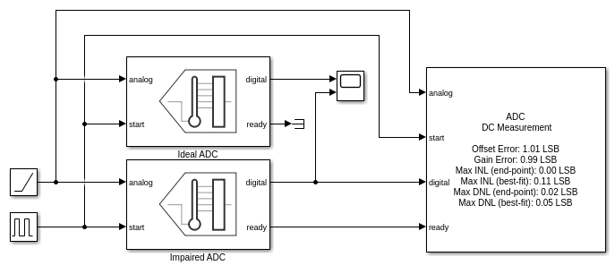
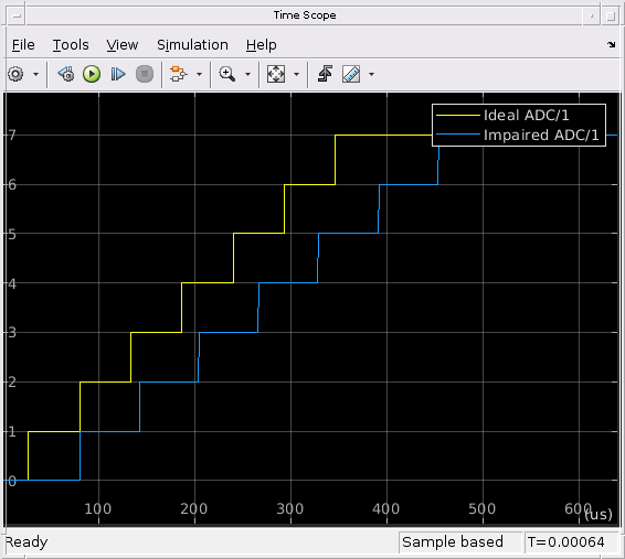
The ADC DC Measurement block confirms the values of the impairments to within a margin of error determined by the sample rate of the system. The offset error and gain error were both entered as1LSB. Offset error was measured as 1.08 LSB and gain error was measured as 0.97 LSB. Errors in these measurements are due to the converter not sampling exactly at its threshold values. The maximum expected error in LSB is:

where is the slope of the input ramp/sawtooth signal in LSB/s, and
 is the ADC's conversion start frequency.
See Also
You can also select a web site from the following list:
Americas
- América Latina(Español)
- Canada(English)
- United States(English)
Europe
- Belgium(English)
- Denmark(English)
- Deutschland(Deutsch)
- España(Español)
- Finland(English)
- France(Français)
- Ireland(English)
- Italia(Italiano)
- Luxembourg(English)
- Netherlands(English)
- Norway(English)
- Österreich(Deutsch)
- Portugal(English)
- Sweden(English)
- Switzerland
- United Kingdom(English)