A field-programmable gate array (FPGA) is an electronic device that includes digital logic circuitry you can program to customize its functionality. Because the logic in the FPGA is programmed specifically to perform your application, it can execute this functionality faster and with less power consumption than software instructions running on a general-purpose application processor. An FPGA that also includes a processor on the device is called a system-on-chip, orSoC FPGA。
How do you program an FPGA?
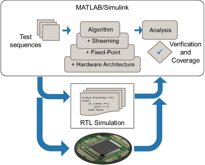
If you are starting from an algorithm in MATLAB®or Simulink®,您将首先需要从刺激和分析中分区设计,定义硬件分区的输入和输出。
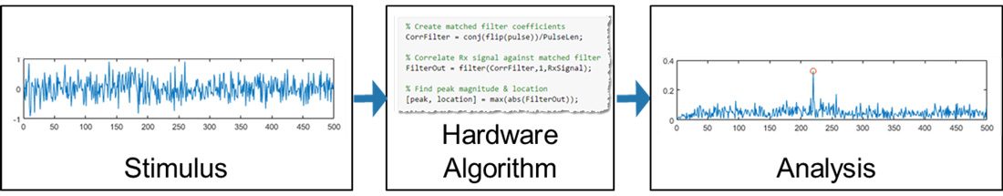
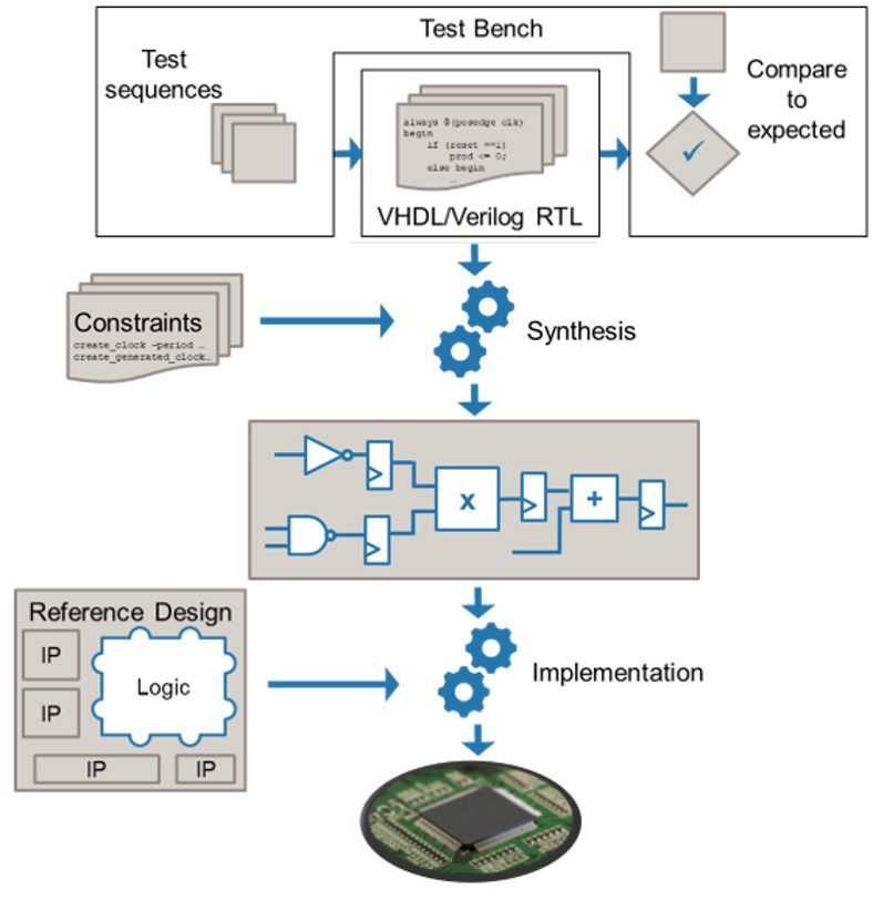
Partitioning the elements of your test bench from the algorithm intended for hardware targeting.
The major steps in FPGA programming are:
- Hardware architecture design.In the case of an SoC FPGA, the hardware-software SoC architecture.
- Design.This is the process of creating the hardware logic itself, typically by writing register-transfer logic (RTL) using a hardware description language (HDL) such as VHDL®或者verilog.®。The goal is to match the functionality of the algorithm while operating on a continuous stream of data, using fixed-point operations for efficiency.
- 验证。This step ensures that the design works as intended before FPGA programming. This can be as simple as aVHDL或Verilog Testbench;商业项目通常使用诸如普遍验证方法的方法(uvm.).
- Synthesis.该技术将RTL转换为数字逻辑门,并尝试满足您的寄存器到寄存器时钟频率目标,同时最大限度地减少FPGA上的资源的使用。
- Integration.FPGA包含许多专用资源已经是引脚,时钟信号,输入/输出处理,例如模数转换器(ADC),以及电路板上的片外存储器的接口。SOC FPGA还具有专用寄存器,即硬件和软件都可以使用彼此通信。您的设计需要插入此“参考设计”。
- Implementation.This is the process of determining which physical resources on the FPGA to program with which logic, and how to connect (route) them. This produces the bitstream that is loaded onto the device for FPGA programming.
- 实验室测试和调试。在FPGA编程之后,您可以使用实际输入或测试输入来运行。第一个尝试通常涉及弄清楚为什么它不起作用以及如何解决它。大部分时间都是由于在验证步骤中未识别的设计步骤中的问题。
A typical workflow from algorithm design to FPGA programming.
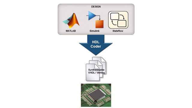
FPGA编程with MATLAB and Simulink
如果您在Matlab和Simulink中绘制算法,则可以专注于设计算法和硬件架构。万博1manbetx使用MATLAB和SIMULINK进行FPGA编程的主要步骤是:万博1manbetx
- 添加硬件架构。You will need to adapt your algorithms to add hardware architecture to process a continuous stream of data, typically withfixed-point data types。Simulink offers a time-based visual environment for硬件architecture design。最好的做法是模拟您的设计版本,并将结果与黄金算法结果进行比较。
- Code generation.一旦您有硬件就绪设计,HDL编码器™使用链接生成独立于无关的Verilog或VHDL RTL,用于调试和可追溯性的模型,以实现功能安全工作流程,如DO-254和ISO 26262。
- Integration.您仍然需要一个用于HDL编码器的参考设计,将算法插入FPGA编程。许多人都可以硬件支持包万博1manbetx, or from your FPGA board vendor.
- Synthesis and implementation.HDL编码器可以生成RTL综合的脚本和项目,它与合成和实施工具集成了Xilinx,Intel,和微笑to provide automated FPGA programming workflows.
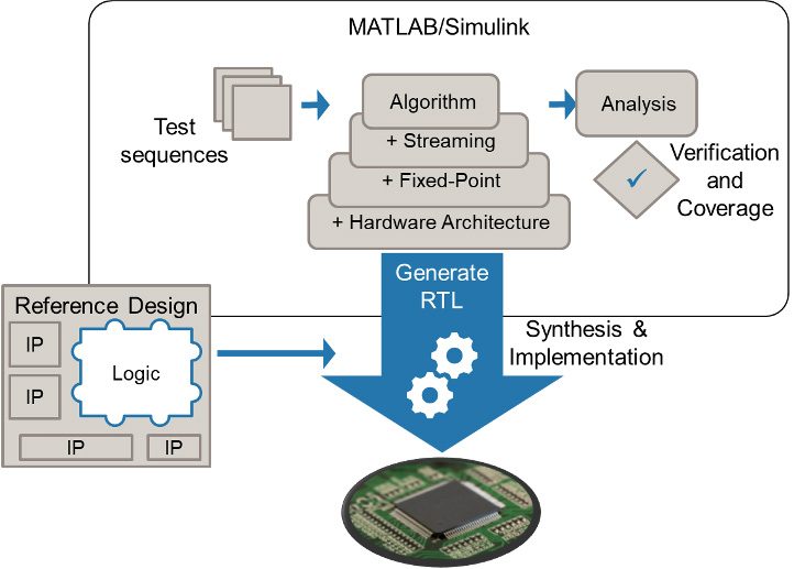
Refining your algorithm with hardware detail, then generating synthesizable RTL to target an FPGA development kit or a custom board.
- 验证。The simplest way to verify that your RTL functions the same as your algorithm is to useHDL Verifier™ to cosimulate the RTL running in Mentor Graphics®Questa®或者®Xcelium™ together with your design and testbench in MATLAB and Simulink. Be sure to test as many scenarios and corner cases as you can before FPGA programming because debugging on the FPGA provides far less visibility and requires longer iterations. You can use万博1manbetxSimulink Test™以编程方式运行和管理您的测试用例,Simulink Coverage™to measure how well you have verified your design.
- 实验室测试和调试。HDL Verifier使您可以将逻辑从MATLAB作为AXI主站插入到FPGA中的数据,并插入逻辑以捕获来自FPGA内部的信号以进行调试。您可以使用Matlab和Simulink直接调万博1manbetx试FPGA,无论您是否正在使用它们,请为您的FPGA编程工作流程使用。
Cosimulating your MATLAB and Simulink together with your implemented design running in a supported simulator or on an FPGA board.